
- English
- Español
- Português
- русский
- Français
- 日本語
- Deutsch
- tiếng Việt
- Italiano
- Nederlands
- ภาษาไทย
- Polski
- 한국어
- Svenska
- magyar
- Malay
- বাংলা ভাষার
- Dansk
- Suomi
- हिन्दी
- Pilipino
- Türkçe
- Gaeilge
- العربية
- Indonesia
- Norsk
- تمل
- český
- ελληνικά
- український
- Javanese
- فارسی
- தமிழ்
- తెలుగు
- नेपाली
- Burmese
- български
- ລາວ
- Latine
- Қазақша
- Euskal
- Azərbaycan
- Slovenský jazyk
- Македонски
- Lietuvos
- Eesti Keel
- Română
- Slovenski
- मराठी
- Srpski језик
中国 CVD sic メーカー、サプライヤー、工場
CVD SiC is a vacuum deposition process used to produce high-purity solid materials. This process is often used in semiconductor manufacturing to form thin films on wafer surfaces. During the chemical vapor deposition (CVD) process for producing silicon carbide (SiC), a substrate is exposed to one or more volatile precursors, which chemically react on the substrate surface to form the desired SiC deposit. Among the various methods for producing SiC, CVD produces products with high uniformity and purity, and offers strong process controllability.
Simply put, CVD SiC refers to SiC produced via the chemical vapor deposition (CVD) process. In this process, gaseous precursors, typically containing silicon and carbon, react in a high-temperature reactor to deposit a thin SiC film onto a substrate. CVD SiC is valued for its exceptional properties, including high thermal conductivity, chemical inertness, mechanical strength, and resistance to thermal shock and wear. These properties make chemical vapor deposited (CVD) silicon carbide (SiC) ideal for demanding applications such as semiconductor manufacturing, aerospace components, armor, and high-performance coatings. This material's exceptional durability and stability under extreme conditions ensure its effectiveness in improving the performance and lifespan of advanced technologies and industrial systems.
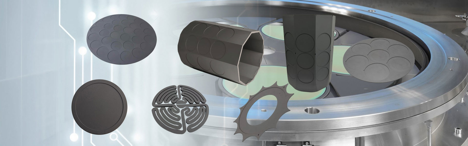
CVD SiC materials, due to their unique combination of excellent thermal, electrical, and chemical properties, are well-suited for applications in the semiconductor industry, where high-performance materials are required. Chemical vapor deposited (CVD) silicon carbide (SiC) components are widely used in etching equipment, MOCVD equipment, Si and SiC epitaxy equipment, and rapid thermal processing equipment.
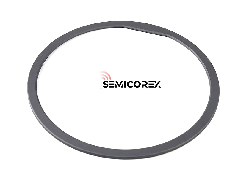
The largest market segment for CVD SiC components is etching equipment components. Due to its low reactivity to chlorine- and fluorine-containing etching gases and its electrical conductivity, CVD silicon carbide (SiC) is an ideal material for components such as focus rings in plasma etching equipment. CVD silicon carbide (SiC) components in etching equipment include focus rings, gas showerheads, trays, edge rings.
Take the focus ring, for example. This critical component is placed outside the wafer and in direct contact with it. Voltage is applied to the ring to focus the plasma passing through it, thereby focusing the plasma on the wafer and improving processing uniformity. Traditionally, focus rings are made of silicon or quartz. However, with the advancement of integrated circuit miniaturization, the demand for and importance of etching processes in integrated circuit manufacturing continues to increase. The power and energy of the plasma used for etching are also increasing, especially in capacitively coupled plasma (CCP) etching equipment, which requires even higher plasma energies. Consequently, focus rings made of silicon carbide are becoming increasingly popular.
Due to the high performance of CVD SiC and its ability to be sliced into very thin sections, it can also benefit sputter targets and all types of electrodes.
Process of Chemical Vapor Deposition (CVD)
CVD is a process that transforms a material from a gas phase to a solid phase, used to form a thin film or coating on a substrate surface. The following are the basic steps in CVD:
1. Substrate Preparation
Choose an appropriate substrate material and perform the appropriate cleaning and surface treating to produce a clean, flat surface with good adhesion.
2. Reactive Gas Preparation
Prepare the necessary amount of reactive gas or vapor and inject it into the deposition chamber by some means (gas supply system). The reactive gas can be an organic compound, a metal-organic precursor, inert gas, or other gaseous species.
3. Deposition Reaction
If all instrumentation is setup correctly the CVD process will begin under the pre-defined reaction conditions. The reactive gas that has been injected into the chamber will undergo some chemical or physical reaction on the substrate surface to form a deposit onto the substrate surface. The deposit formation can be the result of several types of processes depending on the deposition method, these include vapor-phase thermal decomposition, chemical reaction, sputtering, epitaxial growth, etc.
4. Control and Monitoring
At the same time during the deposition process, certain deposition parameters need to be controlled and monitored in real time if the observer wishes to ensure the best possible properties in the film are maintained. These include relevant temperature measurement, pressure monitoring, and regulation of gas flow, all the while aiming to keep the desired reaction conditions stable and constant.
5. Deposition Completion and Post-Processing
When either the deposition time, predetermined thickness, or method selected, is achieved the introduction of the reaction gas can be ceased and deposition process ended. Following the deposition, several pertinent post-processing methods (annealing, structural modifications, surface treatment, etc.) should be performed to improve the film performance/quality.
It's important to note that the specific vapor deposition process can vary depending on the deposition technology, material type, and application requirements. However, the basic process outlined above covers most common vapor deposition steps.


- View as


エッチングエッジリング
Semicorex エッチング エッジ リングは、ウェハ エッジ周囲のプラズマ分布を制御し、エッチングの均一性、プロセス精度、および全体的な半導体製造パフォーマンスを向上させる高純度 CVD SiC プラズマ対向コンポーネントです。 Semicorex は、精密エンジニアリングと信頼性の高い世界供給に支えられ、高度な CVD SiC フォーカス リング、アース リング、シャワーヘッド、カスタマイズされたプラズマ制御コンポーネントを世界中の半導体メーカーに提供しています*。
続きを読むお問い合わせを送信
CVD SiCフィン
Semicorex CVD SiC Fin は、化学気相成長法によって製造された厚く高密度の炭化ケイ素固体コンポーネントであり、卓越した純度、耐久性、耐食性を必要とするプラズマ対向および超高温半導体用途向けに設計されています。 Semicorex は、高度な CVD 炭化ケイ素コンポーネントを世界中の半導体装置メーカーに供給し、最も要求の厳しいプロセス環境向けにカスタマイズされたソリューション、精密エンジニアリング、信頼できるグローバル配信を提供します。
続きを読むお問い合わせを送信
半導体用セラミックフォーカスリング
Semicorex 半導体用セラミック フォーカス リングは、高強度プラズマ エッチング環境向けに特別に設計された CVD SiC 材料から作られた高性能リング部品です。セミコレックスは半導体用CVD SiCセラミックフォーカスリングの業界トップメーカーです。お問い合わせをお待ちしております。
続きを読むお問い合わせを送信
CVD SiC フォーカスリング 2L10-506419-21用
高性能 CVD SiC 材料で作られた Semicorex 2L10-506419-21 用 CVD SiC フォーカス リングは、精密半導体エッチング プロセスで使用される TEL VIGUS RK4 装置用に特別に設計された重要なリング部品です。 Semicorex を選択すると、正確で均一なエッチング結果を達成するための理想的な CVD SiC ソリューションが得られることになります。
続きを読むお問い合わせを送信
固体炭化ケイ素フィン
Semicorex 固体炭化ケイ素フィンは、主に半導体熱処理装置の高温炉で使用される固体 CVD SiC から精密機械加工された高性能部品です。 Semicorex は、市場をリードする品質を備えたカスタム設計の炭化ケイ素フィンを大切なお客様に提供することに尽力しており、中国における長期的なパートナーとなることを楽しみにしています。
続きを読むお問い合わせを送信
Semicorex は CVD sic を長年生産しており、中国のプロの CVD sic メーカーおよびサプライヤーの 1 つです。バルク梱包を提供する高度で耐久性のある製品を購入すると、迅速な配達で大量の製品を保証します。長年にわたり、お客様にカスタマイズされたサービスを提供してきました。お客様は当社の製品と優れたサービスに満足しています。私たちはあなたの信頼できる長期的なビジネスパートナーになることを心から楽しみにしています!私たちの工場から製品を購入することを歓迎します。